
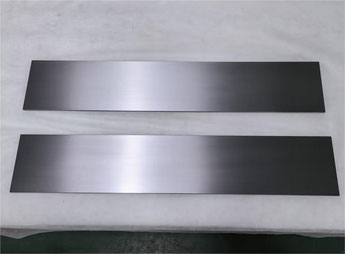
Tantalum (Ta) Target
Tantalum (Ta) target(Tantalum Target) is mainly used in physical vapor deposition (PVD) and chemical vapor deposition (CVD) processes.
Tantalum (Ta) is widely applied in the fields of semiconductor, optics, medical, and aerospace due to its high melting point, corrosion resistance, biocompatibility, and other properties.
1. Characteristics
1) Physical and chemical properties
・High melting point (3017℃)
・Excellent corrosion resistance
・High density (16.6 g/cm³): applicable to high-energy sputtering to increase thin film deposition efficiency.
・Good electrical conductivity: Low resistivity, suitable for semiconductor and electronic device applications.
・Biocompatibility
2) Processing and microstructure
・High purity (≧99.9%~99.999%)
・Uniform grain structure: Grain size is usually controlled to 40-60 μm, ensuring uniformity of sputtered thin film.
・Multiple shapes can be processed
2. Main Applications
1) Semiconductor and microelectronics industries
Integrated Circuit (IC) Barrier Layer: In copper interconnect processing, tantalum thin film prevents copper diffusion and improves chip stability.
・Magnetic storage devices (HDD/MRAM).
・Power semiconductors: electrode materials for high-power devices to improve high-temperature resistance performance.
2) Optical and optoelectronic fields
・Anti-reflective coatings: Used in lenses and filters to increase light transmittance in optical devices.
・Transparent Conductive Oxide (TCO) are used in place of ITO in displays (OLED/LCD) to improve electrical conductivity.
3) Aerospace and high temperature coatings
・Aero engine parts
・Satellite optical lenses: enhance reflectivity and durability.
4) Medical equipment
・X-ray devices
5)Corrosion protection coatings
・Chemical plants
・Marine engineering
株式会社スパッタコア
大阪府大阪市淀川区西中島6丁目3番32号
第2新大阪ビル 707号室
TEL: 06-6-6732-9818
FAX: 06-6-6732-9819
MAIL: ken@ttcm.co.jp
Sputtercore Co. Ltd.
6-3-32 Nishinakajima, Yodogawa-ku, Osaka 532-0011, Japan,
No.2 Shin-Osaka Bldg. Room#707
TEL: +81-6-6732-9818
FAX: +81-6-6732-9819
MAIL: ken@ttcm.co.jp
