
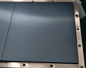
Niobium oxide (Nb₂Ox) target
A high-performance ceramic material with unique physical and chemical properties, widely applied in the fields of semiconductor, optoelectronics, and coating technology.
1. Characteristics
1) High chemical stability
・The material is highly inert to acids, alkalis, and other chemicals at room temperature, making it suitable for corrosive
environments.
2) Excellent electrical performance
・High dielectric constant that makes it an ideal material for semiconductor insulating
layers and gate dielectrics.
・Good electrochemical stability, suitable for energy storage devices such as batteries and capacitors.
3) High melting point (~ 1512°C)
・Suitable for high temperature processes such as PVD (Physical Vapor Deposition) and CVD (Chemical Vapor Deposition), and
withstands high temperatures.
4) Excellent optical performance
・High refractive index and low dispersion properties make it suitable for optical films (filters, antireflection coatings, etc.).
5) High Purity and Denseness
・The purity and density can reach more than 99.9% and 4.47 g/cm³, respectively, ensuring high quality of sputtered thin films.
2. Main Applications
1) Semiconductor industry
・Used to produce high-k insulating layers and improve the performance of integrated circuits.
2) Optoelectronics field
・Optical communication devices (e.g., optical waveguides), optical detectors, display panels (e.g., OLED touch layers).
3) Optical coatings
・Lens coatings, filters, low-emissivity glass (Low-E glass), reducing thermal radiation.
4) High temperature resistant and corrosion resistant coatings
・Aerospace engine coatings, chemical plant protective layers.
5) New energy applications
・Transparent conductive layer of thin film solar cells, increasing photoelectric conversion efficiency.
株式会社スパッタコア
大阪府大阪市淀川区西中島6丁目3番32号
第2新大阪ビル 707号室
TEL: 06-6-6732-9818
FAX: 06-6-6732-9819
MAIL: ken@ttcm.co.jp
Sputtercore Co. Ltd.
6-3-32 Nishinakajima, Yodogawa-ku, Osaka 532-0011, Japan,
No.2 Shin-Osaka Bldg. Room#707
TEL: +81-6-6732-9818
FAX: +81-6-6732-9819
MAIL: ken@ttcm.co.jp
