
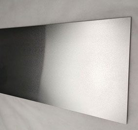
Molybdenum (Mo) target
Mo target is a high-performance sputtering target material and is widely applied to semiconductors, photovoltaics, display panels, aerospace, and other fields due to its high melting point, high electrical conductivity, corrosion resistance, and excellent mechanical performance.
1. Characteristics
1)High melting point and high temperature resistance
・Mo has a melting point of 2620°C, making it suitable for high-temperature sputtering processes such as PVD and CVD.
・Mo has excellent mechanical strength and chemical stability even at high temperatures.
2)Excellent electrical and thermal conductivity
・Electrical conductivity: approx. 1.9 x 10 x S/m (close to 1/3 of copper), suitable for conductive thin films in the electronics industry.
・Thermal conductivity: approx. *138 W/(m-K), useful for heat dissipation during sputtering and enhancing film deposition stability.
3)High purity and denseness
・Purity is usually ≥99.95% (3 N 5), and some high-purity Mo targets can reach 99.99% (4 N).
・Density >99% is generated, and crystal grains are uniform (<20 μm), which reduces particle scattering during sputtering.
4)Good corrosion resistance and anti-oxidation properties.
・Although it is resistant to acid and alkali corrosion at room temperature, it is easily oxidized at high temperatures (>600°C) and must be used in an inert atmosphere or vacuum environment.
5)High mechanical strength and wear resistance.
・The high hardness (HV≈250) and good abrasion resistance make it suitable for high-energy sputtering.
2. Main Applications
1)Semiconductors and integrated circuits
・Conductive layer : Barrier layer for copper interconnections (Cu-Mo) to prevent copper diffusion.
・Electrode materials: Electrode films used in
display panels such as TFT-LCDs and OLEDs.
2)Solar cells (photovoltaic industry)
・Back electrode materials
・Used in CIGS (copper indium gallium selenide) thin film solar cells to increase photoelectric conversion efficiency.
・Transparent Conductive Thin Film (TCO): Used in combination with zinc oxide (ZnO) or indium tin oxide (ITO).
3)Display panel (TFT-LCD, OLED)
・As conductive thin film materials for gate, source and drain.
・Bendable electrodes for flexible displays (because molybdenum thin film has low stress properties).
4)Aerospace and high temperature resistant coatings
・Heat and abrasion resistant coatings for engine blades, rocket nozzles and other high temperature components.
5)Tool coatings and decorative coatings
・Improvement of wear and corrosion resistance of tools and molds.
・Used in wear-resistant coatings for high-end watches and jewelry to enhance luster and durability.
6)Nuclear industry and medical equipment
・Used in X-ray targets and nuclear reactor materials due to its high melting point and low coefficient of thermal expansion.
株式会社スパッタコア
大阪府大阪市淀川区西中島6丁目3番32号
第2新大阪ビル 707号室
TEL: 06-6-6732-9818
FAX: 06-6-6732-9819
MAIL: ken@ttcm.co.jp
Sputtercore Co. Ltd.
6-3-32 Nishinakajima, Yodogawa-ku, Osaka 532-0011, Japan,
No.2 Shin-Osaka Bldg. Room#707
TEL: +81-6-6732-9818
FAX: +81-6-6732-9819
MAIL: ken@ttcm.co.jp
